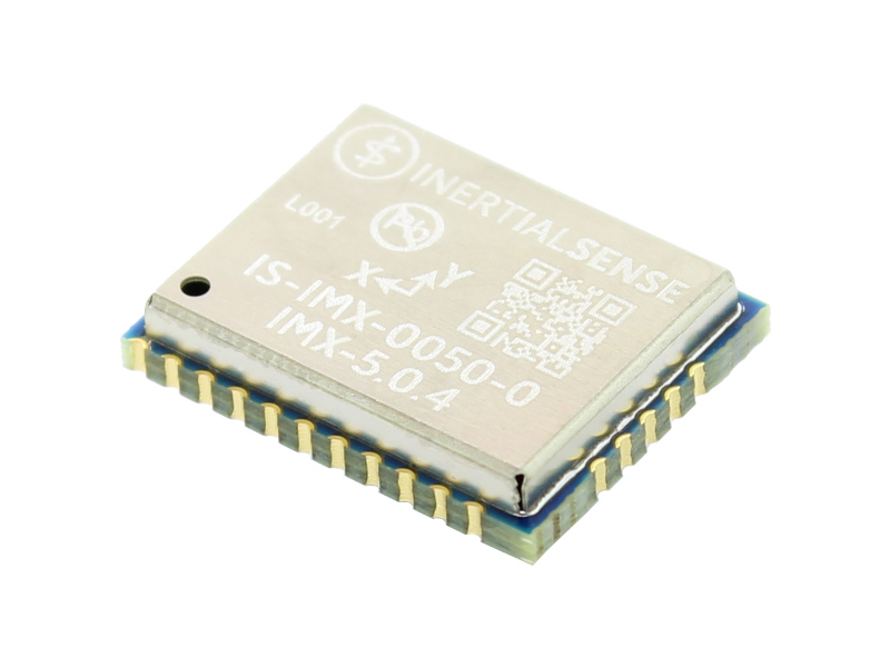
Hardware Integration: IMX-5 Module
Warning
The IMX-5 series of products is approaching its End of Life. Full Notification.
Pinout

| Pin | Name | I/O | Description |
|---|---|---|---|
| 23-29, 31,32 | Not Connected | - | Not connected internally. Connect to ground (GND). |
| 30 | Not Connected | - | Not connected internally. (For IMX-6 compatibility, this pin must be tied to 3.3V to enable IMX-6 USB operation.) |
| 0,11,21 | GND | - | Supply ground |
| 1 | USB_P | I/O | USB Data Positive Line |
| 2 | USB_N | I/O | USB Data Negative Line |
| 3 | VBKUP | I | Connect VBKUP to VCC. |
| 4 | G1/Rx2/RxCAN/SCL | I/O | GPIO1 Serial 2 input (TTL) Serial input pin from CAN transceiver* I2C SCL line |
| 5 | G2/Tx2/TxCAN/SDA/STRB | I/O | GPIO2 Serial 2 output (TTL) Serial output pin to CAN transceiver* I2C SDA line Strobe time sync input |
| 6 | G6/Rx1/MOSI | I/O | GPIO6 Serial 1 input (TTL) SPI MOSI |
| 7 | G7/Tx1/MISO | I/O | GPIO7 Serial 1 output (TTL) SPI MISO |
| 8 | G8/CS/STRB | I/O | GPIO8 SPI CS Strobe time sync input |
| 9 | G5/SCLK/STRB | I/O | GPIO5 SPI SCLK Strobe time sync input |
| 10 | G9/nSPI_EN/STRB/DRDY | I/O | GPIO9 SPI Enable: Hold LOW during boot to enable SPI on G5-G8 Strobe time sync input or output. SPI DRDY alternate pin (active-high: data available when high) |
| 12 | nRESET | I | System reset on logic low. May be left unconnected if not used. |
| 13 | G14/SWCLK | I/O | GPIO14 |
| 14 | G13/XSDA/PPS2/DRDY | I/O | GPIO13 GNSS2 PPS SPI data available when high Alt I2C SDA |
| 15 | G12/XSCL/SWO | I/O | GPIO12 Alt I2C SCL |
| 16 | G11/SWDIO | I/O | GPIO11 |
| 17 | G10/BOOT | I/O | Leave unconnected. BOOT mode used in manufacturing. !!! WARNING !!! Asserting a logic high (+3.3V) will cause the IMX to reboot into ROM bootloader (DFU) mode. |
| 18 | G4/Rx0 | I/O | GPIO4 Serial 0 input (TTL) |
| 19 | G3/Tx0 | I/O | GPIO3 Serial 0 output (TTL) |
| 20 | G15/PPS1 | I | Input for GNSS PPS for time synchronization pulse. |
| 22 | VCC | I | 3.3V supply input |
*External transceiver required for CAN interface.
Application
UART Interface
The following schematic demonstrates a typical setup for the IMX-5 module. If the system processor is not capable of updating the IMX firmware, it is recommended to add a header to an alternate IMX serial port for firmware updates via an external computer. The reset line is not necessary for typical use.

SPI Interface
The SPI interface is enabled by holding the pin 10 low during boot up.

Manufacturing
Soldering
The IMX-5 can be reflow soldered. Reflow information can be found in the Reflow Information page of this manual.
Tape Packaging
The IMX-5 modules are available in cut tape as well as tape and reel packaging. The following image shows the feed direction and illustrates the orientation of the IMX-5 module on the tape:
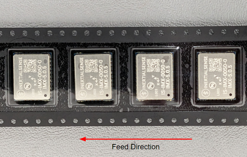 The feed direction to the pick and place pick-up is shown by the orientation of the IMX-5 pin 1 location. With pin 1 location on the bottom of the tape, the feed direction into the pick and place pick-up is from the reel (located to the right of the figure) towards the left.
The dimensions of the tapes for the IMX-5 are shown in the drawing below:
Hardware Design
Recommended PCB Footprint and Layout
A single ceramic 100nF decoupling capacitor should be placed between and in close proximity to the IMX pins 21 and 22 (GND and Vcc). It is recommended that this capacitor be on the same side of the PCB as the IMX and that there not be any vias between the capacitor and the Vcc and GND pins. The default forward direction is indicated in the PCB footprint figure and on the IMX shield as the X axis. The forward direction is reconfigurable in software as necessary.
Design Files
![]()
Open source hardware design files, libraries, and example projects for the IMX module are found at the Inertial Sense Hardware Design repository hosted on GitHub. These include schematic and layout files for printed circuit board designs, and 3D step models of the InertialSense products usable for CAD and circuit board designs.
Reference Design Projects
The EVB-2 and IG-1 circuit board projects serve as reference designs that illustrate implementation of the IMX PCB module.