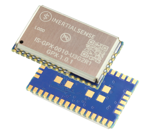
Hardware Integration: GPX-1 Module
Pinout
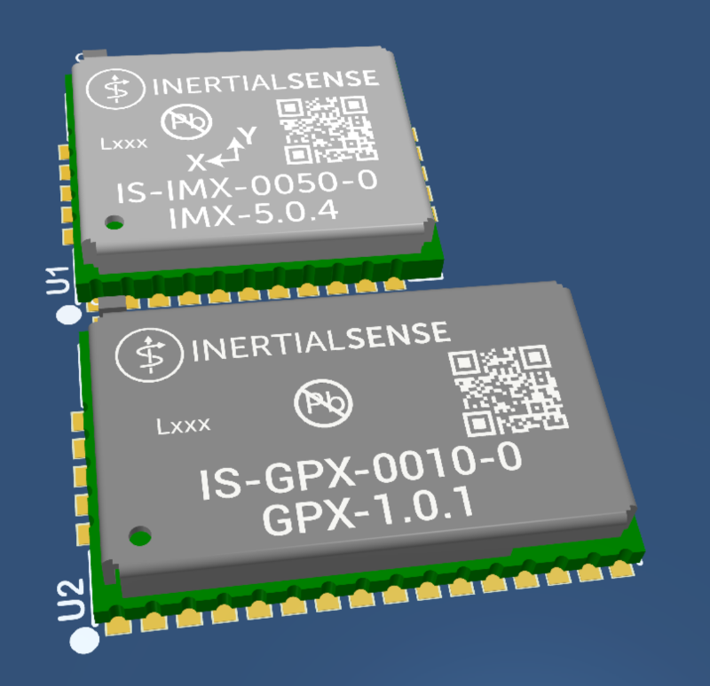
The GPX-1 module footprint and pinout similar that of the IMX-5 such that the common power and interface pins are at the same location. The GPX-1 is extended to accommodate additional GNSS inputs and output. The GPX-1 is designed to work in conjunction with the IMX-5.

| Pin | Name | Type | Description |
|---|---|---|---|
| 33-37 | Not Connected | - | Not connected internally. Connect to ground (GND). |
| 0 | GND | Power | Supply ground on center pads. |
| 11,13,15,31 | GND | Power | Supply ground |
| 1 | USB_P | I/O | USB full-speed Positive Line. USB will be supported in future firmware updates. |
| 2 | USB_N | I/O | USB full-speed Negative Line. USB will be supported in future firmware updates. |
| 3 | VBKUP | Power | Backup supply voltage input (1.75V to 3.6V). Future firmware updates will use voltage applied on this pin to backup GNSS ephemeris, almanac, and other operating parameters for a faster startup when VCC is applied again. This pin MUST be connected to a backup battery or VCC. |
| 4 | G1/Rx2/RxCAN/SCL | I/O | GPIO1 Serial 2 input (TTL) Serial input pin from CAN transceiver* I2C SCL line |
| 5 | G2/Tx2/TxCAN/SDA/STRB | I/O | GPIO2 Serial 2 output (TTL) Serial output pin to CAN transceiver* I2C SDA line Strobe time sync input |
| 6 | G6/Rx1/MOSI | I/O | GPIO6 Serial 1 input (TTL) SPI MOSI |
| 7 | G7/Tx1/MISO | I/O | GPIO7 Serial 1 output (TTL) SPI MISO |
| 8 | G8/CS/STRB | I/O | GPIO8 SPI CS Strobe time sync input |
| 9 | G5/SCLK/STRB | I/O | GPIO5 SPI SCLK Strobe time sync input |
| 10 | G9/nSPI_EN/STRB/DRDY | I/O | GPIO9 SPI Enable: Hold LOW during boot to enable SPI on G5-G8 Strobe time sync input or output. SPI data ready alternate location |
| 12 | GNSS1_RF | I | GNSS1 antenna RF input. Use an active antenna or LNA with a gain of 15-25dB. Place the LNA as close to the antenna as possible. Filtered 3.3V from VCC is injected onto the pad to power active antennas (power injection can be disabled in software). Connect to ground with 5V-14V TVS diode for ESD and surge projection (e.g. Littlefuse PESD0402-140). |
| 14 | GNSS2_RF | I | GNSS2 antenna RF input. Same requirements as GNSS1_RF |
| 16 | VCC_RF | O | Supply output for GNSS active antenna. Connect VCC_RF through 33-120nH inductor (e.g. Murata LQW15ANR12J00D, 110mA max) to GNSS1_RF and GNSS2_RF to inject DC supply for active antenna(s). VCC_RF is supplied from VAUX through an onboard 1A load switch and 10 ohm resistor. Disable by setting GPX_SYS_CFG_BITS_DISABLE_VCC_RF (0x00000001) in DID_GPX_FLASH_CFG.sysCfgBits. |
| 20 | G20/LNA-EN | I/O | GPIO20 |
| 21 | GNSS2_PPS | O | GNSS2 PPS time synchronization output pulse (1Hz, 10% duty cycle) |
| 22 | nRESET | I | System reset on logic low. May be left unconnected if not used. |
| 23 | G14/SWCLK | I/O | GPIO14 |
| 24 | G13/DRDY/XSDA | I/O | GPIO13 SPI Data Ready Alt I2C SDA |
| 25 | G12/XSCL | I/O | GPIO12 Alt I2C SCL |
| 26 | G11/SWDIO | I/O | GPIO11 |
| 27 | G10/BOOT | I/O | Leave unconnected. BOOT mode used in manufacturing. !!! WARNING !!! Asserting a logic high (+3.3V) will cause the IMX to reboot into ROM bootloader (DFU) mode. |
| 28 | G4/Rx0 | I/O | GPIO4 Serial 0 input (TTL) |
| 29 | G3/Tx0 | I/O | GPIO3 Serial 0 output (TTL) |
| 30 | GNSS1_PPS | O | GNSS1 PPS time synchronization output pulse (1Hz, 10% duty cycle) |
| 32 | VCC | Power | 1.8V to 3.3V supply input. |
| 38 | G16/QDEC0.A | I/O | GPIO16 |
| 39 | G17/QDEC0.B | I/O | GPIO17 |
| 40 | VAUX | Power | Input supplies for the USB and VCC_RF (GNSS antenna supply). Connect to +3.3V (3.0V to 3.6V) to supply USB and VCC_RF. Can be left floating if USB or VCC_RF are not needed. |
| 41 | G18/QDEC1.A | I/O | GPIO18 |
| 42 | G19/QDEC1.B | I/O | GPIO19 |
*External transceiver required for CAN interface.
Application
GNSS-INS Block Diagram

Typical Application: GPX-1 IMX-5
The following schematic shows the recommended interconnection for the GPX-1 and IMX-5. To enable GNSS PPS1 and PPS2 time synchronization input on the IMX-5 the corresponding enable bits must be set in DID_FLASH_CONFIG.ioConfig and DID_FLASH_CONFIG.ioConfig2.

| Designator | Manufacturer | Part Number | Description |
|---|---|---|---|
| D1, D2 | Littlefuse | PESD0402-140 | TVS DIODE 14VWM 40VC 0402 |
| I1, I4 | Murata | LQW15ANR12J00D | FIXED IND 120NH 110MA 2.66OHM SM |
Layout Guidance
GNSS_RF Trace
The GNSS_RF trace should be designed to work in the combined GNSS L1 + L5 signal band.
For FR-4 PCB material with a dielectric permittivity of for example 4.2, the trace width for the 50 Ω line impedance can be calculated.
A grounded co-planar RF trace is recommended as it provides the maximum shielding from noise with adequate vias to the ground layer.
The RF trace must be shielded by vias to ground along the entire length of the trace and the ZEDF9P RF_IN pad should be surrounded by vias as shown in the figure below.
[INSERT LAYOUT FIGURE HERE]
Design Guidance
Backup Battery
For achieving a minimal Time To First Fix (TTFF) after a power down (warm starts, hot starts), make sure to connect a backup battery to V_BCKP.
- Verify your battery backup supply can provide the battery backup current specified in the ZEDF9P datasheet.
- Allow all I/O including UART and other interfaces to float/high impedance in battery backup mode (battery back-up connected with VCC removed).
RF Front-end Circuit Options
Important
Active antenna(s) are required for the GPX-1.
Manufacturing
Soldering
The GPX-1 can be reflow soldered. Reflow information can be found in the Reflow Information page of this manual.
Tape Packaging
The GPX-1 modules are available in cut tape as well as tape and reel packaging. The following image shows the feed direction and illustrates the orientation of the GPX-1 module on the tape:
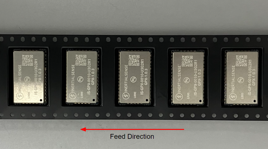 The feed direction to the pick and place pick-up is shown by the orientation of the GPX-1 pin 1 location. With pin 1 location on the bottom of the tape, the feed direction into the pick and place pick-up is from the reel (located to the right of the figure) towards the left.
The dimensions of the tapes for the GPX-1 are shown in the drawing below:
Hardware Design
Recommended PCB Footprint and Layout
A single ceramic 100nF decoupling capacitor should be placed between and in close proximity to the module pins 31 and 32 (GND and Vcc). It is recommended that this capacitor be on the same side of the PCB as the GPX and that there not be any vias between the capacitor and the Vcc and GND pins.
Design Files
![]()
Open source hardware design files, libraries, and example projects for the GPX module are found at the Inertial Sense Hardware Design repository hosted on GitHub. These include schematic and layout files for printed circuit board designs, and 3D step models of the InertialSense products usable for CAD and circuit board designs.
Reference Design Projects
Coming soon