Hardware Integration: IG-2 (IMX5 + GPX1)
Warning
The IMX-5 series of products is approaching its End of Life. Full Notification.
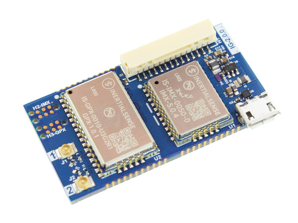
The Inertial Sense IG-2 is a PCB module with IMX-5 and GPX-1 multi-frequency GNSS receiver.
- Surface mount reflowable.
- Onboard dual GNSS for simultaneous RTK positioning and GPS compassing.
- Micro USB and 14 pin I/O header for convenient evaluation.
Connecting Your Unit
For the purposes of basic evaluation, the easiest interface available on the IG-2 is by using a micro-USB cable. A cable included in the evaluation kit. The cable provides power and communications with the installed module via USB virtual communications port.
Pinout
Module Pinout

Header H1 Pinout
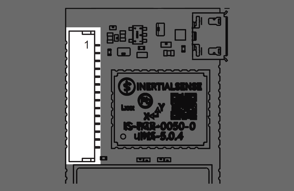
The IG-2 module and IG-2 header H1 have the same pinout assignment for pins 1-14. Because H1 only has 14 pins, pins 15 and above listed in the following table are only on the IG-2 module.
| IG-2 Module & IG-2 H1 Pin |
Name | I/O | Description |
|---|---|---|---|
 1 1 |
GND | PWR | - |
| 2 |
VIN | PWR | 4V-20V supply voltage input |
 3 3 |
+3.3V | PWR | Regulated 3.3V supply input/output. |
| 4 |
Reserved | Not Connected | |
 5 5 |
G1/Rx2/RxCAN/SCL | I/O | IMX GPIO1 Serial 2 input (TTL) Serial input pin from CAN transceiver* I2C SCL line6 |
 6 6 |
G2/Tx2/TxCAN/SDA/STROBE | I/O | IMX GPIO2 Serial 2 output (TTL) Serial output pin to CAN transceiver* I2C SDA line Strobe time sync input |
 7 7 |
G3/Tx0 | I/O | IMX GPIO3 Serial 0 output (TTL) |
 8 8 |
G4/Rx0 | I/O | IMX GPIO4 Serial 0 input (TTL) |
 9 9 |
G5/SCLK/STROBE | I/O | IMX GPIO5 SPI SCLK Strobe time sync input |
 10 10 |
G6/Rx1/MOSI | I/O | IMX GPIO6 Serial 1 input (TTL) SPI MOSI |
 11 11 |
G7/Tx1/MISO | I/O | IMX GPIO7 Serial 1 output (TTL) SPI MISO |
 12 12 |
G8/CS/STROBE | I/O | IMX GPIO8 SPI CS Strobe time sync input |
| 13 |
G9/nSPI_EN/STROBE /STROBE_OUT/SPI_DRDY |
I/O | IMX GPIO9 SPI Enable: Hold LOW during bootup to enable SPI on G5-G8 Strobe time sync input or output. SPI data ready alternate location. |
| 14 |
GPS.TIMEPULSE | O | GPS PPS UTC time synchronization signal. |
| 15 | GND | PWR | - |
| 16 | VBAT | I/O | GPS backup supply voltage. (1.4V to 3.6V) enables GPS hardware backup mode for hot or warm startup (faster GPS lock acquisition). MUST connect GPS_VBAT to VCC if no backup battery is used. |
| 17 | G10/BOOT_MODE | I/O | Leave unconnected. IMX BOOT MODE used in manufacturing. !!! WARNING !!! Asserting a logic high (+3.3V) will cause the IMX to reboot into ROM bootloader (DFU) mode. |
| 18 | G11 | I/O | IMX GPIO11 |
| 19 | G12 | I/O | IMX GPIO12 GPS reset |
| 20 | G13/DRDY | I/O | IMX GPIO13 SPI data ready |
| 21 | G14/SWCLK | I/O | IMX GPIO14 |
| 22 | nRESET | I | System reset (IMX and GPX) on logic low. May be left unconnected if not used. |
| 23 | GND | PWR | - |
| 24 | USB_N | I/O | IMX USB Data Negative Line |
| 25 | USB_P | I/O | IMX USB Data Positive Line |
| 26 | GPX_G16/QDEC0A | I/O | GPX GPIO16 |
| 27 | GPX_G17/QDEC0B | I/O | GPX GPIO17 |
| 28 | GPX_G18/QDEC1A | I/O | GPX GPIO18 |
| 29 | GPX_G19/QDEC1B | I/O | GPX GPIO19 |
| 30 | +3.3V | PWR | Regulated 3.3V supply input/output. |
| 31 | GPX_G10_BOOT | I/O | GPX GPIO10 |
| 32 | GPX_G5/SCLK | I/O | GPX GPIO5 GPX SPI clock |
| 33 | GPX_G6/Rx1/MOSI | I/O | GPX GPIO6 GPX Serial 1 input (TTL) GPX SPI MOSI |
| 34 | GPX_G7/Tx1/MISO | I/O | GPX GPIO7 GPX Serial 1 output (TTL) GPX SPI MISO |
| 35 | GPX_G8/CS | I/O | GPX GPIO8 GPX SPI chip select |
| 36 | GPX_G9/SPI_EN | I/O | GPX GPIO9 GPX SPI Enable: Hold LOW during bootup to enable SPI on G5-G8 |
| 37-47 | GND | PWR | - |
Schematic
Hardware Design
Recommended PCB Footprint and Layout
The default forward direction is indicated in the PCB footprint figure and on the silkscreen as the X axis. The forward direction is reconfigurable in software as necessary.
Soldering
The IMX-5 can be reflow soldered. Reflow information can be found in the Reflow Information section of this manual.
Design Files
![]()
Open source hardware design files, libraries, and example projects for the IMX module are found at the Inertial Sense Hardware Design repository hosted on GitHub. These include schematic and layout files for printed circuit board designs, and 3D step models of the InertialSense products usable for CAD and circuit board designs.
Reference Design Projects
The EVB-2, IG-1, and IG-2 circuit board projects serve as reference designs that illustrate implementation of the IMX PCB module.
Related Parts
| Part | Manufacturer | Manufacturer # | Description |
|---|---|---|---|
| H1 | JST | GHR-14V-S | 14 pin connector 1.25mm pitch for IMX I/O connection. |